
NEWS DETAIL

How are Industrial Quartz Blanks Made?
High-purity quartz is the foundation for semiconductor and photovoltaic applications.
The process starts with selecting ultra-pure quartz sand, which is then melted and refined to remove impurities such as metals and hydroxyl groups.
The molten quartz is carefully cast into quartz blanks, sometimes using the flame fusion or hydrothermal growth method.
These blanks are the starting point for precision machining and must meet strict chemical and structural standards.

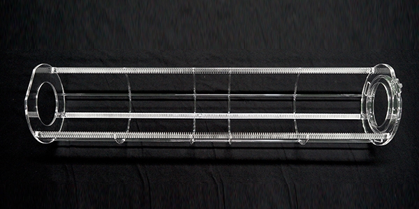
How is Quartz Cut and Shaped Precisely?
Quartz machining relies on CNC cutting and shaping techniques to achieve the desired dimensions and geometric tolerances.
Diamond-coated tools are commonly used because quartz is extremely hard and brittle.
Careful planning of feed rates, spindle speed, and cooling methods prevents cracks and microfractures.
This stage ensures that each quartz component is ready for subsequent grinding and polishing without structural damage.
What Grinding Methods Ensure Accurate Quartz Parts?
Grinding is critical for refining the dimensions and flatness of quartz components.
Common methods include surface grinding, double-side grinding, and lapping.
These processes remove minor surface imperfections left from cutting and prepare the quartz for optical polishing.
Maintaining tight tolerances during grinding is essential for semiconductor wafers and photovoltaic glass substrates, where even micrometer deviations can affect performance.
How is Quartz Polished to Optical Quality?
Polishing transforms quartz surfaces to optical-grade smoothness, essential for light transmission in semiconductor and PV applications.
Techniques include mechanical polishing with diamond slurries, chemical polishing, and sometimes flame polishing for specialized components.
The goal is to achieve surfaces with minimal roughness and no micro-cracks, ensuring maximum transparency and reducing stress points that could cause breakage.
How Is Quartz Quality Checked After Machining?
After machining and polishing, quality inspection is critical. Techniques include visual inspection, interferometry, surface roughness measurement, and chemical purity analysis.
These inspections verify that the quartz meets both dimensional tolerances and optical clarity standards.
Consistent quality control ensures reliability in sensitive applications like semiconductor wafers and photovoltaic panels.